
Negative-voltage EOS: the supply that went below its own ground
Units come back from the field with the touch controller destroyed. The obvious suspect is a discharge on the touch lines, so the argument becomes which protection device to fit. Then somebody scopes a returned unit while it is running, with nobody touching it, and finds -3.26 V on the 3.3 V rail.

What was being built
A capacitive touch panel on a consumer product. The touch controller sits out on a flex tail, and four lines run back to the host: the two I2C lines, an interrupt and a reset, plus a 3.3 V supply and ground. Ordinary pull-ups on the host side. Across those four lines sits a low capacitance ESD array, referenced to the 3.3 V rail and to ground, which is exactly the part you would fit and exactly where you would fit it.
The same board also drives a speaker. That sentence turns out to matter more than everything before it.
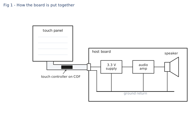
What came back from the field
This was never a production problem. Boards passed test, shipped, and came back weeks later with the touch function dead. Analysis found the controller destroyed, with damage on the supply and on the bus pins.
The natural reading is ESD. People touch this product all day, so a destroyed touch controller looks like a discharge that got past the protection. That reading sends the entire investigation to the protection device: is it fast enough, is the clamping voltage low enough, is it close enough to the connector. Every one of those is a reasonable question. Every one of them turned out to be about the wrong component.
The clue that changed everything
Somebody stopped asking how it failed and went and measured a returned unit while it was running. The capture that came back was taken with the product playing audio at maximum volume, and with nobody touching the panel.
It is worth being careful about what that does and does not establish. It does not prove that playback is the only condition that misbehaves, and nobody has yet reproduced the destruction on the bench. What it does prove is that the product generates a supply excursion far outside the controller’s rating with no user involvement at all.
That is enough to move the investigation off the protection device. A discharge needs a charged object arriving at the port. Nothing arrives at the port here. If the disturbance is present while nobody is touching the product, the energy is coming from inside the product, and audio playback is a clue about where, not the definition of the problem.
What the scope showed
Four channels: the 3.3 V rail, the two bus lines and the interrupt. Playing at full volume, nobody touching anything.
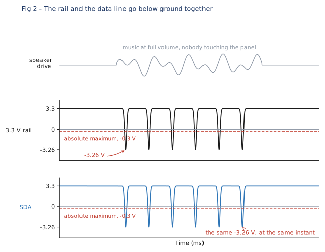
Two things in that capture decide everything that follows.
- The excursions reach -3.26 V. That is not a small undershoot. It is very nearly a whole rail below ground.
- They appear on the 3.3 V rail and on the data line at the same instant, with the same amplitude.
The second point is the important one. An electrostatic discharge on a data line appears on that data line. It does not appear on the supply rail at the same moment with the same amplitude, and it does not repeat in time with a piece of music. What this capture shows is the whole local supply going below the ground it is being measured against.
The number that matters is -0.3 V, not -3.3 V
Every conversation about this failure used "3.3 V, plus or minus 5 percent". That is the operating range, and it is the wrong number for a failure discussion. The number that decides whether the part survives is the absolute maximum rating, and for this controller it is -0.3 V to 3.63 V.
Look at how lopsided that is. Above the rail there is 330 mV of headroom. Below ground there is 300 mV, and that is all. This is not a quirk of one part either: on almost every CMOS datasheet the negative absolute maximum is -0.3 V or -0.5 V, no matter how high the positive rating goes.
So the safe operating area is not symmetrical, and the narrow side is the one nobody checks. The measured event is about ten times past it.
What that does inside the chip
Every pin on a CMOS chip carries two diodes that were never drawn on your schematic. One runs from the pin up to the supply rail. The other runs from ground up to the pin. In normal operation the pin sits somewhere between ground and the rail, so both are reverse biased and neither does anything at all.
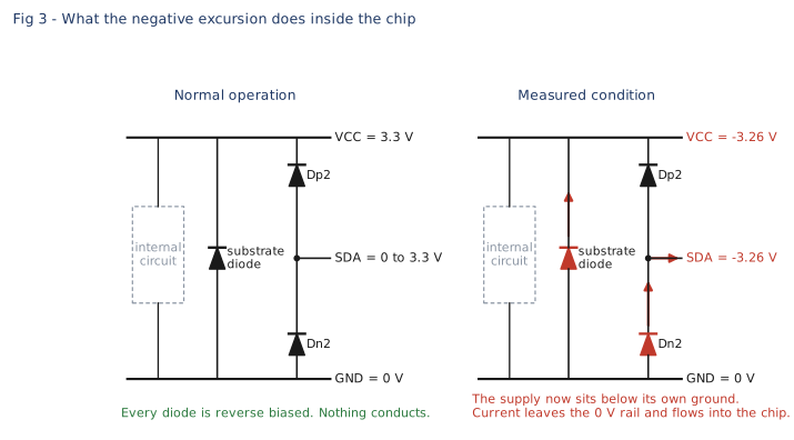
Now hold ground at 0 V and put the supply and the pin at -3.26 V. Two things conduct.
The first is the lower pad diode. Its anode is on ground and its cathode is on the pin, so it is now forward biased by more than 3 V. It conducts hard, limited only by whatever resistance happens to be in the loop.
The second is worse. In a p-substrate CMOS process the substrate is tied to ground and the n-wells are tied to the supply, and that junction is a diode with its anode on ground. When the supply falls below ground, that junction is forward biased across the whole die. The chip is not taking a spike on one pin. It is being supplied backwards.
That is why the damage was not confined to one pin, and it is why the customer’s own analysis reached the right conclusion before anybody talked about protection parts: past roughly 0.3 V of reverse voltage the transistors and diodes inside the chip go into forward conduction. Repeat that at audio rate for a few weeks and you get exactly what came back from the field.
The first proposal
The first suggestion to arrive was a low capacitance unidirectional protection device across the line. The argument for it is simple and it sounds right: a unidirectional device is a plain forward diode in the negative direction, so anything below about -0.7 V turns it on and the line is held at -0.7 V instead of -3.26 V. Roughly a fivefold improvement, from a part that costs very little and adds almost no capacitance.
Why clamping at -0.7 V does not save a part rated to -0.3 V
Before taking that apart, the case for the unidirectional device deserves to be stated properly, because it is a real one. Against a genuine negative ESD transient, on a line that only ever carries positive signals, a unidirectional part is the better choice, and for exactly the reason given: it conducts at about -0.7 V, where a bidirectional part with a 5 V standoff waits until roughly -6 V. That is not one vendor’s opinion, it is the standard industry guidance, and on a normal design it is advice worth following.
The question is whether that reasoning survives being carried onto this failure. It does not, for three reasons, and none of them is a flaw in the general advice. They are things the general advice never had to consider.
The first is the target. Take the forward voltage off a datasheet rather than out of memory. An ultra low capacitance unidirectional device of this class specifies 0.6 V minimum, 0.85 V typical, 1.0 V maximum, and only at 15 mA. The familiar "0.7 V" is a textbook approximation, not a specification. Against a -6 V alternative, 0.85 V is an excellent result. Against an absolute maximum of -0.3 V it is not: the clamp lands at roughly three times the number you needed, with the chip still outside its rating and its own junction still conducting. It also gets worse the harder it works, because forward voltage rises with current, which is exactly why that same datasheet carries a forward clamping voltage versus current curve. Better is not the same as safe.
The second is the one that usually gets missed. The external diode is not in front of the on-chip diode. It is in parallel with it.
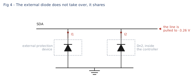
Both have their anode on ground and their cathode on the line. Adding a diode beside a diode does not remove current from the first one, it divides the current between them, and the division is set by their two forward characteristics. For the external part to carry essentially all of it, it has to turn on at a clearly lower voltage than the diode already inside the chip, and a small low capacitance die is not obviously the one that turns on lower. That is a comparison worth making on the bench before you rely on it, because until it is made, "the external part protects the internal one" is an assumption rather than a result.
The third is duration, and it is the one that separates the two situations completely. That device is characterised for a discharge that is over in a hundred nanoseconds, or for a surge lasting a few tens of microseconds. Held at -0.7 V for a hundred nanoseconds, a handful of times, it is doing its job perfectly. Held there in time with a piece of music, for the working life of the product, it is doing something no line on its datasheet describes.
Why our own answer does not help either
This is the part we would normally leave out of an article like this, so it goes near the front instead.
The part we would reach for on a 3.3 V bus is a bidirectional device with a 5.5 V standoff. In our own line that is PS0522G-F4, and in almost every other situation it is the right call. On this failure it does nothing whatsoever. Its breakdown voltage is 6.2 V minimum, so it stays off until the line reaches -6.2 V at the earliest. The event is -3.26 V. It sits inside the window, the device never turns on, and the excursion passes straight through it at 0.1 microamps of leakage.
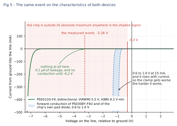
So the unidirectional part clamps to a voltage that still destroys the chip, and the bidirectional part does not clamp at all. Unidirectional against bidirectional was the argument everybody was having, and it was the wrong argument. Neither answer addresses the failure. Recommending ours would have sold a part and left the customer with the same return rate.
There is one more thing in that schematic worth noticing. The array fitted to this board is referenced to the 3.3 V rail, which is normally exactly what you want. But when the rail itself goes to -3.26 V, the reference the array clamps to has gone with it. A rail referenced array is only ever as good as its rail.
When a clamp does help: read the pin's own rating first
Everything above rests on one number, the -0.3 V absolute maximum. That is the normal figure on a CMOS datasheet and it was the right figure for this controller, but it is an assumption doing a great deal of work. It is worth separating the general rule from this particular board, because the general rule is the useful part.
The question is not whether a clamp helps. It is whether the clamp lands inside the pin's own absolute maximum, and that depends on a number printed in the datasheet of the chip you are protecting rather than on anything about the protection device.
- Pin rated to about -0.3 V. This is the common case and it is the one above. A silicon junction conducts at roughly 0.7 V and the voltage rises with current, so even a perfect forward clamp lands at more than twice the limit. No protection part fixes it, and the answer is the ground return.
- Pin rated to -2 V or -3 V. Some rugged industrial and automotive I/O genuinely do specify this, and it is worth reading rather than assuming. Here a unidirectional device conducting below a volt sits comfortably inside the rating, and it really is the right fix.
So the first thing to do on a board like this is not to choose a protection part. It is to open the absolute maximum table of the chip behind the port and read the negative row. That one number decides which of the two situations you are in, and the two have opposite answers.
Where the rating does allow it, on a 3.3 V rail the part is PT0389J-D1U. It is unidirectional with a 3.3 V standoff, and it is a power line device rather than a signal line one, which is what a rail wants. Above zero it does nothing until breakdown. Below zero there is no TVS action at all: it is a plain forward diode, which is exactly the behaviour that helps here.
One caveat survives in both cases, and it is the duration argument from earlier. Even where the clamp lands inside the rating, a protection device is characterised for a discharge lasting nanoseconds or a surge lasting microseconds. It is not characterised for something that repeats in time with a piece of music for the working life of the product. In that situation a clamp buys margin, and the source of the excursion still has to be fixed.
ESD, EOS and surge are three different problems
These get treated as one topic because the same component sits in the same place for all three. They are not one topic.
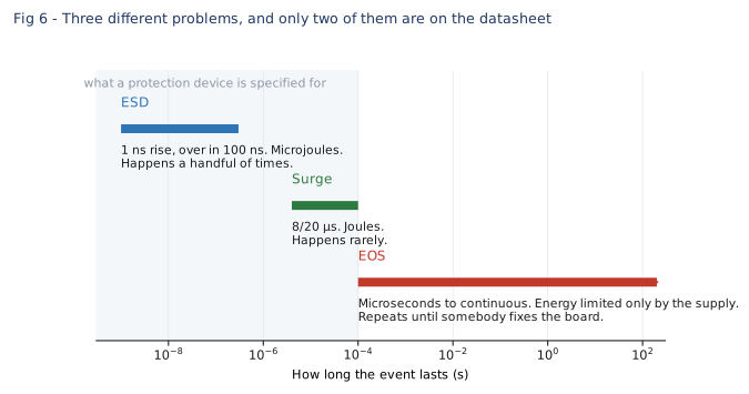
- ESD is a nanosecond event. About 1 ns of rise, over in roughly 100 ns, a few millijoules at most, and it happens a handful of times in the life of a product. An 8 kV contact discharge under IEC 61000-4-2 comes from a 150 pF source, which is 4.8 mJ of stored energy.
- Surge is a microsecond event. The 8/20 µs waveform, joules rather than millijoules, and rare.
- EOS is not an event at all. It is a condition. It can last microseconds or for ever, its energy is limited only by whatever is supplying it, and it repeats until somebody changes the board.
Put a number on the third one. Suppose the on-chip diode carries only 100 mA at 3.26 V. Nobody measured the real current and 100 mA is a deliberately modest guess. That is still 0.33 W, so one second of it is 0.33 J, which is about seventy times the energy of a single 8 kV contact discharge. Every second, for as long as the music plays.
A protection device datasheet describes the first two categories. It does not describe the third, and no combination of numbers on it will tell you whether the part survives a condition it was never characterised for.
Where a negative rail comes from
A supply that goes below its own ground is almost always one of three things.
- Something inductive being switched off. Current in an inductor cannot stop instantly. A speaker coil, a motor, a solenoid or a relay will push the node driving it below ground when the drive turns off. How far below depends on how fast the drive stops and on what is there to catch it.
- A shared return path. A large load current flowing in copper that also carries the digital ground develops a voltage across that copper. Circuits at the far end see their whole reference move. Nothing on the schematic hints at this, because on the schematic every ground is the same node.
- A rail that gets pulled down and rings. A large current step ending into a rail with thin bulk capacitance and a long path back to the supply will undershoot, and if that loop is inductive enough the undershoot goes below zero.
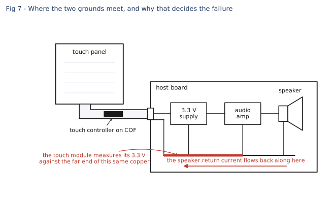
That is the same drawing you started with, and nothing has been moved. All that has been added is a mark on one piece of copper, which is exactly how this failure hides. On a schematic every ground symbol is the same node, so the second mechanism is invisible: there is literally nothing to see. On the physical arrangement it is obvious. The touch module sits at the far end of a piece of copper that a large audio current is flowing through, and the further along that copper it sits, the further its reference can move.
The fourth possibility, an event arriving through the connector, is the one everyone assumes first and it is the one this capture rules out. It repeats with the audio, and it happens with nobody touching the product.
Which of the first three it is decides the fix, and one capture taken with one ground reference cannot tell them apart. That is the next piece of work, not a thing to guess at.
Which products this shows up in
This one arrived on a touch panel, but nothing about it is specific to touch. Any board that puts a switching or inductive load next to low voltage logic can do the same thing. The ones we see most often:
- Audio. Speaker outputs and class-D amplifiers in TVs, soundbars, smart speakers, tablets and handsets. The speaker coil is an inductor and the currents are large.
- Motor drive. Brushed and BLDC motors, fans and pumps in appliances, power tools, robot vacuums and industrial equipment. Every commutation is a switched inductor.
- Relays and solenoids. Coils in smart meters, access control, vending, HVAC and factory automation. The classic negative kick, and the classic missing freewheel diode.
- LED backlight and LED driver boards. Boost and buck-boost stages in monitors, signage and instrument clusters, especially with PWM dimming, which turns the whole load on and off thousands of times a second.
- Hot plug and cable connect. USB, Type-C, docking connectors and battery packs, where a connection is made live and the rail moves before it settles.
- Automotive and industrial 12 V and 24 V boards. Long harnesses, shared grounds between modules and inductive loads on the same supply.
The line that connects all of them is not the application, it is the layout question underneath it: does a large switched current share copper with the ground that your logic is measured against? If it does, the rail can move, and the protection on your data lines is not what decides whether the board survives.
What to measure next
Four measurements, in this order. None of them needs new hardware.
- Move the scope ground. Take the same capture with the ground lead on the touch module’s own ground instead of the host’s. If the -3.26 V disappears, the rail did not go anywhere: the two grounds moved apart from each other, and this is a return path problem.
- Measure the two grounds against each other. Module ground on one channel, host ground as the reference. Whatever appears there is the part of the problem that no device on a signal line can reach.
- Add the speaker current as another channel. If the negative excursion lines up with the moment the drive current changes fastest rather than with peak volume, the mechanism is inductive and it is happening at switch-off.
- Look at the amplifier’s own supply at the same instant. If it shows the mirror image, the disturbance is arriving through the supply and the touch module is a bystander.
That is an afternoon of work, and it decides which of the fixes below is the real one. Skipping it is how a product ends up with three different protection parts fitted across three revisions and the same return rate at the end of it.
What actually fixes it
In order of how much good they do.
- Stop the two grounds moving relative to each other. Give the speaker its own return to the supply so that the audio current does not share copper with the digital ground. Where the module is on a flex tail, add ground conductors and shorten the loop. This is layout work, and in the next revision it is free.
- Put the bulk capacitance at the amplifier, not back at the connector. A rail that does not sag has nothing to ring back from.
- Add series resistance on the signal lines. This does not fix the rail and it is no substitute for the first two, but it limits how much current the on-chip diode has to carry when the rail does move. On a bus with kilohm pull-ups, a hundred ohms or so costs very little. Check it against the low level output budget and the bus timing before committing to a value.
- If the rail can still be driven below ground after all that, catch it with a part built for continuous current. A Schottky from ground to the rail, cathode on the rail, starts conducting a few hundred millivolts below zero. Even that lands around 0.3 to 0.5 V, so treat it as the backstop that turns a fatal excursion into a survivable one, not as permission to skip the first two.
Notice what is not on that list for a pin rated to -0.3 V: a different ESD array. Nothing clamps below a diode drop, so on that pin no array, ours or anybody else’s, turns a -3.26 V rail into a safe one. If the chip you are protecting is rated to -2 V or -3 V, the arithmetic changes and a unidirectional part does land inside the rating, which is the case set out above.
An ESD device protects against ESD
That is not a tautology, it is the whole point. A protection device is characterised for a specific waveform, a specific duration and a specific number of repetitions. Outside those, it has no defined behaviour at all. It is not a general safety net for anything unpleasant that happens to a pin.
So when a board is dying, the question to ask is never "which protection part should I fit". It is three other questions: what is the event, how long does it last, and where is the energy coming from. Answer those and the right component, or the right piece of layout, is usually obvious. Skip them and you can spend a year changing a part that was never in the path.
On this board the answer to the third question was: from inside the product, out of its own speaker. No component on the touch lines was ever going to fix that, and saying so was worth more to the customer than selling them one.
The short version
- If a board fails while nobody is touching it, the energy is coming from inside the product. It is not ESD.
- Survival is decided by the absolute maximum rating, not the operating range. On the negative side that is usually only -0.3 V.
- A forward diode clamps at 0.6 to 1.0 V, and higher as the current rises, so it cannot protect a pin rated to -0.3 V. It also sits in parallel with the chip’s own diode and merely shares the current.
- Read the negative absolute maximum of the chip you are protecting before choosing anything. At -0.3 V no clamp lands inside the rating and the fix is the ground return. At -2 V or -3 V a unidirectional part does land inside it and is the right answer.
- A bidirectional device whose standoff is wider than the event never conducts at all. Check that the event is outside the window before assuming the part does anything.
- If the rail moves as well as the signal, nothing on the signal line can help. Fix the return path first.